


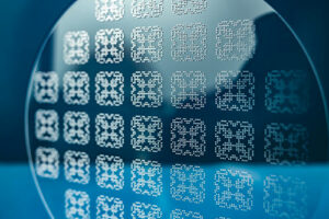
Electron beam lithography (EBL) is a versatile patterning technique based on electron beam technology that enables mask-less (“direct-write”) lithography of electron-sensitive materials.
It is possible to overcome the diffraction limit of the UV lithography with sub-nm feature resolution. The machine is essentially composed by an electron column for the generation of the beam with controlled aperture, a high-precision stage for the positioning of the samples with very low stitching errors. EBL is the flexible instrument that gives fast results in the designing phase of new projects and can be used for small volume production thanks to high speed patterning.
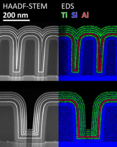
 Atomic Layer Deposition (ALD) is an advanced chemical vapour deposition technique that allows ultra-thin films to be deposited in a precisely controlled way. The precursors are sequentially inserted inside the chamber and react with the surface to be deposited autonomously in sequence. For each gas pulse in the chamber, a reaction will occur and therefore the deposition of a nanometric film will cover the surface homogeneously layer by layer. Not only does ALD provide excellent thickness control and uniformity but 3D structures can be covered with a conformal coating for high-aspect-ratio structures.
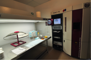
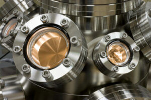
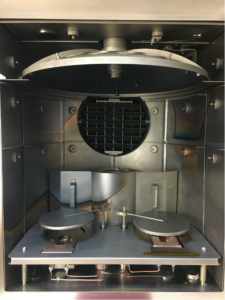 OAC-75F machine situated in CNOS laboratory of nanophotonics allows, via e-beam evaporation, the deposition of layers of different kind of materials, from oxides (as SiO2, HfO2, Al2O3), to metals (as Au, Al, Ti), to semiconductors (as Silicon), in a high vacuum chamber. This machine has been customized and optimized in order to achieve a high degree of accuracy, up to 1-2 Å in the nominal thickness, and a surface roughness of 0.1nm for most materials, in order to be able to reliably fabricate also layers with thickness at the nanometer scale. The presence of two e-beam guns and two sets of crucibles for target materials allows an efficient fabrication also of multilayer structures with two or more different materials. Furthermore, with a suitable programming of the two e-beam guns, it is possible to evaporate at the same time two different materials with different deposition rates, in order to obtain an arbitrary amorphous mixture of two materials. To guarantee a high level of adhesion and/or compactness of materials, it is possible to program the activation, before and during the deposition, of a plasma ion source based on Argon and/or Oxygen gases. The large vacuum chamber allows to allocate, for the same deposition process, several substrates of different shape and dimensions, from standard silicon wafers to optical fibers, providing a very good level of uniformity thanks to the rotation of the dome hosting the substrates.

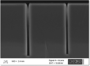
 Reactive Ion Etching – RIE – is a chemical etching technique that uses a plasma to remove a material from a substrate. The plasma is generated by an electromagnetic field in a high vacuum chamber starting from precursors in a gaseous state. The ions present in the plasma chemically attack the surface and react with it. The result is a very uniform surface and it is possible to control the process very well thanks to various parameters involved in the process, such as temperature, flow of gases.
The use of this machine is intended for the effective and selective removal of material from substrates on which deposition and / or lithography operations have already been performed. The system allows to work on conventional planar substrates and on unconventional substrates such as optical fibers. For example, it is possible to attach the glass of which the optical fiber is made in a suitable way downstream of a lithographic process. In this way only the exposed areas will be etched and it will therefore be possible to create nanostructures with very high aspect ratios.
 The femtosecond laser system, a proper laser laboratory on an optical table, is a versatile system that allows ablation of glass, metals and polymers, and photolithography using the common photoresist. Thanks to the four-axis (XYZ and one of rotation R), we can process several types of substrates – from planar surfaces to unconventional surfaces, like optical fiber tip – with extreme resolution and accuracy avoiding sample damaging.
Among the various fields of application, some examples are:
 The two-photon polymerization system (2PP) is a maskless lithography system, designed for the fabrication of high-resolution 2D and 3D structures. This machine has a galvanomentric system that allows us to manufacture nanostructures with desired geometry straight on both planar and non-planar surfaces. It has an X and Y resolution of 400nm and a scan speed of up to 100mm / s.
The 2PP system has different application area:
Laser system: NIR femtosecond laser
Type of resins: PDMS, biocompatible and non-cytotoxic according to ISO 10993-5, with high refractive index (n = 1.62) and low autofluorescence.
 The Raith eLINE Plus electron beam system is the most versatile nanolithography system for a wide range of applications across all scientific disciplines, and now in its third generation, it is effectively an evolution of the world’s best-selling EBL system. The Raith eLINE Plus system is an advanced platform for electron beam lithography (EBL) and nanometric engineering, designed for high-resolution nanofabrication applications. This tool combines electron lithography functionality with high-resolution imaging, manipulation, and material deposition on a nanometer scale.
The Raith eLINE Plus is an advanced electron beam lithography (EBL) system designed for high-precision nanofabrication applications. This tool offers a beam resolution of less than 1.6 nm, allowing the creation of structures with line widths under 5 nm, with precision that ensures alignment between successive layers with a standard deviation of 40 nm. It can operate at acceleration voltages ranging from 0.5 kV to 30 kV, adapting to different materials and resist thicknesses.
 The system is equipped with a laser interferometer that controls the stage movement over a 100 mm x 100 mm working area, with positioning accuracy in the nanometer range. Thanks to advanced techniques like electron beam-induced deposition (EBID) and electron beam-induced etching (EBIE), it is possible to create three-dimensional structures and locally modify the properties of materials, opening up a wide range of applications in nanoengineering.
The Raith eLINE Plus leverages proprietary technologies such as the “Fixed Beam Moving Stage” (FBMS) and “Modulated Beam Moving Stage” (MBMS), which enable continuous writing without stitching errors, making this system particularly suited for the creation of extended structures like waveguides or periodic gratings. The sample loading system features a load lock, allowing for quick insertion and extraction, reducing downtime and minimizing the risk of contamination.
Moreover, the system integrates In-lens and SE2 detectors for high-resolution imaging, facilitating inspection and alignment during lithography processes. The Raith eLINE Plus is a versatile and highly precise solution for research and production of nanometer-scale devices, offering reliability and high performance in advanced nanofabrication applications.
 The PlasmaPro 100 Cobra by Oxford Instruments is an advanced reactive ion etching (RIE) system, designed to deliver high performance in nanofabrication applications, including MEMS devices, optoelectronics, and power electronics. Utilizing a high-density inductively coupled plasma (ICP), the system achieves high etching rates, high selectivity, and low-damage processes while maintaining excellent uniformity.
The system is compatible with wafers up to 200 mm, supporting both single-wafer and batch processing. The PlasmaPro 100 Cobra is designed for exceptional versatility, allowing the use of a wide range of reactive gases, including CHF3, CF4, O2, Ar, Cl2, CH4, H2, and N2, enabling a variety of etching processes. This system features an electrode with a broad temperature range from -150°C to 400°C, which can be regulated through a cooling system using liquid nitrogen, a recirculating fluid chiller, or resistive heating.
Another key feature of the PlasmaPro 100 Cobra is its ability to maintain a low chamber pressure, utilizing high gas flow rates and a high degree of conductance to ensure uniform delivery of reactive species to the substrate. This approach enables wide process windows, making the system suitable for a broad range of advanced applications.
For optimal temperature control, the system is equipped with an electrode regulated by a recirculating fluid chiller, ensuring precise temperature management during etching. Additionally, it features an in-situ laser monitor that continuously observes the wafer reflectivity, allowing optimal etching process control and endpoint detection. An in-situ optical emission monitor enables plasma spectroscopy, monitoring the chamber cleaning process endpoint, improving process repeatability and quality.
The PlasmaPro 100 Cobra is designed to ensure excellent uniformity and high precision, with low-damage etching capabilities, making it an ideal solution for fabricating advanced nanometer-scale devices.
In summary, the key technical features of the PlasmaPro 100 Cobra are:
The PlasmaPro 100 Cobra by Oxford Instruments is an advanced reactive ion etching (RIE) system, designed to deliver high performance in nanofabrication applications, including MEMS devices, optoelectronics, and power electronics. Utilizing a high-density inductively coupled plasma (ICP), the system achieves high etching rates, high selectivity, and low-damage processes while maintaining excellent uniformity.
The system is compatible with wafers up to 200 mm, supporting both single-wafer and batch processing. The PlasmaPro 100 Cobra is designed for exceptional versatility, allowing the use of a wide range of reactive gases, including CHF3, CF4, O2, Ar, Cl2, CH4, H2, and N2, enabling a variety of etching processes. This system features an electrode with a broad temperature range from -150°C to 400°C, which can be regulated through a cooling system using liquid nitrogen, a recirculating fluid chiller, or resistive heating.
Another key feature of the PlasmaPro 100 Cobra is its ability to maintain a low chamber pressure, utilizing high gas flow rates and a high degree of conductance to ensure uniform delivery of reactive species to the substrate. This approach enables wide process windows, making the system suitable for a broad range of advanced applications.
For optimal temperature control, the system is equipped with an electrode regulated by a recirculating fluid chiller, ensuring precise temperature management during etching. Additionally, it features an in-situ laser monitor that continuously observes the wafer reflectivity, allowing optimal etching process control and endpoint detection. An in-situ optical emission monitor enables plasma spectroscopy, monitoring the chamber cleaning process endpoint, improving process repeatability and quality.
The PlasmaPro 100 Cobra is designed to ensure excellent uniformity and high precision, with low-damage etching capabilities, making it an ideal solution for fabricating advanced nanometer-scale devices.
In summary, the key technical features of the PlasmaPro 100 Cobra are:
The PlasmaPro 100 Cobra is a versatile and powerful machine for applications requiring high-precision ion etching on large wafers, with excellent process management capabilities and consistent quality.
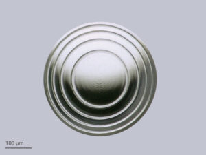
 The Photonic Professional GT2 by Nanoscribe is one of the most advanced 3D printers in the field of microfabrication, designed to produce three-dimensional structures with unparalleled precision and detail. This system is based on two-photon polymerization (2PP) technology, which enables the creation of microscopic-scale objects with extremely high printing resolutions. It is widely used across various sectors, including scientific research, advanced prototyping, and the fabrication of photonic devices, MEMS, and nanotechnology components.
The Photonic Professional GT2 offers a printing resolution down to 160 nm, allowing the creation of extremely small and detailed structures with an unprecedented level of precision in 3D printing. The minimum feature size achievable is 200 nm, making it ideal for applications requiring nanometer-level resolution. This system is perfect for manufacturing complex devices, such as micro-optical systems, photonic microstructures, plasmonic devices, and MEMS.
The build volume of the Photonic Professional GT2 is 100 mm³, allowing the fabrication of structures up to 10 mm x 10 mm x 1 mm. This makes the system suitable for medium-volume prototyping and the creation of complex 3D structures, though the maximum dimensions are smaller compared to large-format 3D printers. The printing speed is another impressive feature of this system: it can operate at speeds of up to 10 mm/s, enabling the rapid production of highly intricate models without compromising print quality. This makes it highly effective for rapid prototyping applications where speed is a critical factor.
The system supports a wide range of photopolymeric materials, which can be selected based on specific design requirements. The resins used for printing are developed to optimize two-photon polymerization, ensuring excellent adhesion and outstanding quality in fine detail reproduction. The versatility in materials allows for a broad range of applications, such as the development of micro-optical devices, sensors, and microfluidic components.
Additionally, the Photonic Professional GT2 is equipped with a highly intuitive management software that simplifies the entire workflow, from CAD design to final printing. The software includes advanced features that optimize the printing process, refine 3D models, and ensure the best possible results without requiring complex interventions.
The main technical features of the Photonic Professional GT2 include:
The Photonic Professional GT2 by Nanoscribe is one of the most advanced 3D printers in the field of microfabrication, designed to produce three-dimensional structures with unparalleled precision and detail. This system is based on two-photon polymerization (2PP) technology, which enables the creation of microscopic-scale objects with extremely high printing resolutions. It is widely used across various sectors, including scientific research, advanced prototyping, and the fabrication of photonic devices, MEMS, and nanotechnology components.
The Photonic Professional GT2 offers a printing resolution down to 160 nm, allowing the creation of extremely small and detailed structures with an unprecedented level of precision in 3D printing. The minimum feature size achievable is 200 nm, making it ideal for applications requiring nanometer-level resolution. This system is perfect for manufacturing complex devices, such as micro-optical systems, photonic microstructures, plasmonic devices, and MEMS.
The build volume of the Photonic Professional GT2 is 100 mm³, allowing the fabrication of structures up to 10 mm x 10 mm x 1 mm. This makes the system suitable for medium-volume prototyping and the creation of complex 3D structures, though the maximum dimensions are smaller compared to large-format 3D printers. The printing speed is another impressive feature of this system: it can operate at speeds of up to 10 mm/s, enabling the rapid production of highly intricate models without compromising print quality. This makes it highly effective for rapid prototyping applications where speed is a critical factor.
The system supports a wide range of photopolymeric materials, which can be selected based on specific design requirements. The resins used for printing are developed to optimize two-photon polymerization, ensuring excellent adhesion and outstanding quality in fine detail reproduction. The versatility in materials allows for a broad range of applications, such as the development of micro-optical devices, sensors, and microfluidic components.
Additionally, the Photonic Professional GT2 is equipped with a highly intuitive management software that simplifies the entire workflow, from CAD design to final printing. The software includes advanced features that optimize the printing process, refine 3D models, and ensure the best possible results without requiring complex interventions.
The main technical features of the Photonic Professional GT2 include:
In conclusion, the Photonic Professional GT2 by Nanoscribe is a highly advanced and versatile solution for 3D microfabrication, delivering superior performance in high-precision and high-detail structure manufacturing, making it ideal for scientific research, advanced prototyping, and various nanotechnology applications.
 The Zeiss Gemini 1 Sigma 300 VP is an advanced scanning electron microscope (SEM) designed to provide high-resolution imaging and detailed elemental analysis of samples in variable pressure (VP) mode. This instrument is ideal for applications requiring precise surface characterization and chemical composition analysis, such as materials research, nanotechnology, and materials science.
The Zeiss Gemini 1 Sigma 300 VP is a next-generation scanning electron microscope (SEM) that delivers advanced performance in the characterization of samples at both microscopic and nanoscopic levels, utilizing variable pressure (VP) mode. This system is designed for precise analysis of morphology and chemical composition, with a particular focus on sensitive or non-conductive samples, such as biological, soft, or delicate materials that might be damaged during conventional preparation. It is used across various sectors, including materials research, nanotechnology, materials science, and electronic engineering.
 One of the main features of the Sigma 300 VP is the innovative Gemini 1 optics, which combines magnetic and electrostatic fields to control and optimize electron focusing, reducing sample distortion and enhancing image quality. Thanks to this optical system, the microscope can operate at both low and high voltages without compromising resolution. The Gemini 1 optics allows for high-resolution imaging, even on challenging samples such as magnetic or conductive materials, with a resolution of 1.2 nm at 15 kV and 2.2 nm at 1 kV.
Another key feature of the Sigma 300 VP is its variable pressure (VP) mode, which enables scanning without requiring pre-processing steps such as metallization, which could alter the sample structure. VP mode is particularly useful for non-conductive or environmentally sensitive samples, as it allows controlled pressure conditions within the chamber, preserving the original characteristics of the specimen. This makes it particularly valuable for analyzing biological materials, polymers, and other soft materials requiring delicate handling.
The Sigma 300 VP is equipped with an advanced detection system that includes multiple detectors to gather various aspects of the sample. The in-lens secondary electron (SE) detector provides detailed surface topography, while the angle-selective backscattered electron (BSE) detector delivers information on the elemental composition of materials. The combination of these detectors allows for surface analysis at different depths, yielding precise insights into element distribution.
Regarding spatial resolution, the Sigma 300 VP supports a wide range of accelerating voltages, from 0.02 kV to 30 kV, enabling a variety of applications. Higher voltages allow for greater penetration depth, while lower voltages provide superior resolution, making them ideal for thin or low-conductivity samples. This flexibility in voltage selection enhances scanning capabilities, producing sharp and detailed images with optimized contrast and visibility of microscopic features.
The microscope also features a 5-axis motorized sample stage that enables precise sample manipulation during analysis. This configuration allows users to move the sample along the X, Y, and Z axes, tilt, and rotate it to capture images from different angles, facilitating 3D analysis and the mapping of extended sample areas. This motorization increases efficiency and flexibility, making it easier to analyze samples of various shapes and sizes.
The system is supported by advanced management software that streamlines the entire process of image acquisition, analysis, and visualization. The software includes tools for image manipulation, dimension measurement, quantitative chemical composition analysis, and 3D visualization, reducing operation time and increasing productivity. The software is designed to be intuitive, allowing even less experienced users to achieve high-quality results.
In summary, the Zeiss Gemini 1 Sigma 300 VP is a highly sophisticated scanning electron microscope that offers advanced imaging performance, elemental analysis capabilities, and exceptional operational flexibility. Its high resolution, variable pressure mode, broad range of accelerating voltages, and precise sample manipulation make it ideal for applications demanding the highest quality in structural and chemical analysis, such as advanced scientific research, nanotechnology, and materials engineering.
 The Osiris UNIXX SP20 is an advanced photolithography system designed for precision applications in microelectronics, nanotechnology, and other research and development fields. This tool has been developed to meet the needs of laboratories requiring high-quality deposition and development of photosensitive resins on substrates of various sizes and materials.
The system features an intuitive touch screen interface, allowing users to easily manage all process operations. Its graphical interface simplifies access to different operating modes and enables quick configuration of process parameters, reducing the time needed to execute operations and improving overall work efficiency. Machine management via a touchscreen interface also ensures greater precision in controlling process parameters.
One of the distinctive aspects of this system is its ability to handle up to six different process chemicals, allowing for a wide range of applications, including deposition, exposure, and removal of photosensitive resins. This capability makes the Osiris UNIXX SP20 extremely flexible, enabling users to customize the process according to specific project requirements. The ability to use multiple chemicals simultaneously is particularly useful for applications requiring a quick transition between processes without compromising quality or consistency. The system is designed to support substrates up to 8 inches (approximately 200 mm), which are the standard sizes in the microelectronics industry. This allows for the processing of commonly used wafers, ensuring compatibility with most photolithography and microfabrication applications. Although the system supports larger wafers, it can also handle smaller substrates, adapting to various user needs.
Another important feature of the Osiris UNIXX SP20 is the encoded rotation motor, which ensures extraordinary precision in resin deposition. The encoded motor allows for accurate control of speed and positioning during the spin-coating process, ensuring that the resin is evenly distributed across the entire substrate surface. This is crucial for achieving a homogeneous and repeatable layer of photosensitive material, which is essential for successful photolithography processes.
Additionally, the system comes with chucks of various sizes, including 4″ and 5″ mask plates, 3″ and 4″ wafers, and supports for smaller substrates. This feature enhances the system’s versatility, as users can process a variety of substrates, from larger to smaller ones, using a single machine. The ability to easily switch between different chucks allows for process optimization based on the type of substrate and the specific application.
Overall, the Osiris UNIXX SP20 is a highly precise and versatile machine that offers advanced management of photolithography processes. With its intuitive interface, multi-chemical handling capability, ability to process substrates of various sizes, and precise rotation motor, it is particularly suited for research and development applications, prototyping, and small-scale production. Its flexibility and ability to adapt to different types of applications make it an excellent option for professionals in the microelectronics and nanotechnology fields.
 The FemtoLAB by WOP (Workshop of Photonics) is an advanced workstation designed for femtosecond laser micromachining applications. This system is particularly suitable for research and development laboratories, prototyping, and the production of micro- and nanostructured components. Thanks to its ability to operate on a wide range of materials with submicron precision, it is used in numerous fields such as microelectronics, nanotechnology, and photonics.
One of the distinctive features of FemtoLAB is its ability to perform femtosecond laser processing with submicron resolution, enabling the creation of highly precise structures with minimum feature sizes of 200 nm. The system integrates a high-end femtosecond laser, ensuring high power and optimal pulse control, allowing for extremely precise processing without damaging the surrounding material. Thanks to its high pulse frequency and the ability to generate extremely short laser pulses, the FemtoLAB can perform high-speed processing with minimal heat generation, reducing the risk of material alterations.
 To optimize processing precision and speed, the FemtoLAB is equipped with high-performance galvanometric scanners, enabling fast and accurate laser scanning across the sample surface. These scanners are particularly useful for complex processing tasks such as multiphoton polymerization (MPP), direct laser writing (DLW), and laser grooving. The synchronization between sample movement and laser pulse emission is managed with great efficiency, ensuring precise and repeatable results.
The system is controlled by dedicated software, which coordinates all aspects of the processing, from laser emission to sample movement, allowing for comprehensive and intuitive process management. The software is designed to let users customize processing parameters and execute complex operations, combining additive and subtractive processes within a single platform.
The FemtoLAB is highly valued for its versatility, as it enables the combination of additive and subtractive processes within a single machine, eliminating the need for multiple separate pieces of equipment. This feature enhances operational efficiency, reduces preparation time, and optimizes production costs. The system is capable of processing a variety of materials, including metals, polymers, glass, ceramics, and composite materials.
The machine is designed to be modular and scalable, easily adapting to new applications and processes. Additionally, the comprehensive support provided by WOP, including system installation and training, ensures the rapid and optimal integration of the FemtoLAB into laboratories and research centers. Its versatility and ease of use also make it particularly useful for rapid prototyping applications.
Finally, numerous prestigious research centers and universities worldwide have chosen the FemtoLAB for its performance and reliability. For example, it has been used by the Centre technologique Optique & Lasers ALPhANOV in Bordeaux, the University of Applied Sciences in Upper Austria, and the Technische Universität Berlin for advanced projects in photonics and nanotechnology.
In summary, the FemtoLAB by WOP is a highly advanced and versatile solution for femtosecond laser micromachining, offering precision, flexibility, and power within a single platform. Its ability to process various materials while combining additive and subtractive processes makes it ideal for advanced research applications and the prototyping of microscopic and nanoscopic devices.